nextnano3 - Tutorial
next generation 3D nano device simulator
1D Tutorial
Applying the NEGF method to a quantum well
Author:
Stefan Birner,
Tillmann
Kubis
If you are interested in the input files that are used within this tutorial, please
submit a support ticket.
-> 1DNEGF_InGaAs_QW_ballistic_CBR.in - nextnano3
input file using the CBR method
-> 1DNEGF_InGaAs_QW_ballistic.in -
-> 1DNEGF_InGaAs_QW_scattering.in -
-> 1DNEGF_InGaAs_QW_scattering_bias.in -
Applying the NEGF method to a quantum well
This tutorial is based on the following paper:
[Kubis_HCIS14_2005]
Self-consistent quantum transport theory of carrier capture in
heterostructures
T. Kubis, A. Trellakis, P. Vogl
Proceedings of the 14th International Conference on
Nonequilibrium Carrier Dynamics in Semiconductors, M. Saraniti and U.
Ravaioli, eds., Chicago, USA, July 25-19, 2005, Springer Proceedings in
Physics, vol. 110, pp. 369-372
Quantum well structure - InGaAs/GaAs n-i-n heterostructure
- 12 nm In0.14Ga0.86As QW in the center surrounded
on each side by GaAs barriers (of width 19 nm each)
z-coordinates = 19.0d0  31.0d0
	! 19 - 31 [nm]
- Doping: n-i-n
GaAs n-i-n structure with an InGaAs quantum well within the intrinsic
region.
- 0 nm - 17 nm:
- 17 nm - 33 nm:
- 33 nm - 50 nm:
- T = 300 K (room temperature)
- device length = 50 nm
 z-coordinates = 0.0d0  50.0d0
	! 0 - 50 [nm]
- constant effective electron mass throughout the device (parabolic
dispersion): m* = 0.067 m0 (GaAs)
 conduction-band-masses = 0.067d0
	0.067d0  0.067d0 ! [m0]
electron mass of GaAs
To keep this tutorial as simple as possible, we use here the GaAs mass also
for the InGaAs QW.
- Dielectric constants
 static-dielectric-constants  = 12.93d0
	12.93d0 12.93d0 !
epsilon(0)
 optical-dielectric-constants = 10.89d0
	!
To keep this tutorial as simple as possible, we use here the GaAs values
also for the InGaAs QW.
- constant polar optical phonon energy throughout the device: 0.035 eV
(GaAs)
LO-phonon-energy = 0.035d0 ! [eV]
- GaAs/In0.14Ga0.86As conduction band offset: CBO =
0.150 eV
(For simplicity, we do not take into account strain.)
- Grid resolution: 1 nm, i.e. 49 grid points in total (plus the two
boundary points).
This corresponds to 50 equidistant grid points within the NEGF part.
- Ohmic contacts: The two reservoirs at the left and right boundaries are
in thermal equilibrium.
Ballistic NEGF calculation
-> 1DNEGF_InGaAs_QW_ballistic.in
- VSD = 0 eV
(source-drain), see Fig. 1 (a) in
[Kubis_HCIS14_2005]
- ballistic device (absence of any scattering)
- electron-electron scattering in Hartree approximation, see Fig. 1 (a) in
[Kubis_HCIS14_2005]
Necessary feature for ballistic calculation
 $scattering-mechanisms

  ...

  ballistic
= yes      !
Fig.
1(a): switch off scattering (ballistic calculation) - to make calculation faster
Doping profile
The following figure shows the doping profile of the structure.
The structure is n-type doped (n = 1 * 1018 cm-3) with a
16 nm intrinsic region in the center.
The conduction band edge is also indicated to indicate the position of the 12 nm
wide InGaAs quantum well.
The output for the doping profile can be found in the following files:
- doping_concentration1D.dat - doping profile as specified in input
file for each doping function
- doping_profile1D.dat -
- NEGF/dopingV_new.dat -

Conduction band edge
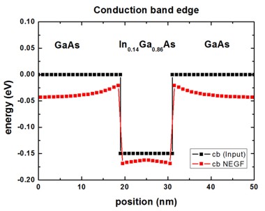
The following figure shows the conduction band edge energy of the GaAs/InGaAs
heterostructure.
The black line is the band edge that is input for the calculation. It
can be found in this file:
NEGF/ex_potential_new.dat (in units of [eV])
The red line is the self-consistently
calculated conduction band profile (calculated by NEGF method) and can be found
in this file:
NEGF/pot_new.dat (in units of
[eV])
Note: The conduction band edge of nextnano³ is usually contained in this
file:
band_structure/cb1D_001.dat (in units of [eV])
(or)
Energy-resolved electron density
The following figure on the left shows the contour plot of the local,
energy-resolved electron density n as a function of position z and
energy E at zero bias and in the absence of any scattering (ballistic
device) for the n-i-n GaAs structure with an InGaAs quantum well in the center.
n(z,E) is in units of [1018 eV-1cm-3].
Integrating n(z,E) over the energy E yields the electron
density n(z).
The black line shows the self-consistently calculated conduction band
edge profile.
The figure on the right shows a contour plot of the energy-resolved local
density of states LDOS(z,E) in units of [eV-1 Angstrom-1].
The LDOS(z,E) is known as the spectral function.
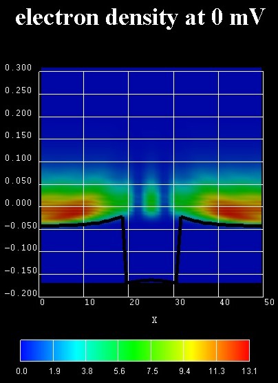 
The zero of energy is put at the Fermi level of the left contact.
In the calculation, the Hartree Coulomb interaction was taken into account
(Poisson equation).
Due to the absence of inelastic scattering, the carriers cannot fill the
quantum well but occupy a resonance that is derived from the third quantum well
state. This explains the interference pattern in the well region at room
temperature.
The energy-resolved electron density n(z,E) can be found
in this file:
NEGF/density_energy_resolved.fld - in units of
[1018 cm-3 eV-1]
(AVS format)
NEGF/density_Ez_energy_resolved.fld - in units of
[1018 cm-3 eV-1]
(AVS format)
   NEGF/spectral_real_avs.fld
-
in units of [eV-1 Angstrom-1] (AVS
format)
   NEGF/pot_avs.fld
-
in units of [eV]
(AVS format)
   NEGF/pot_new.dat
-
in units of [eV]
NEGF calculation including scattering - zero bias (equilibrium)
-> 1DNEGF_InGaAs_QW_scattering.in
Acoustic (both, elastic and inelastic) and polar-optical phonon scattering, electron-electron scattering in
Hartree approximation, see Fig. 1 (b) and 2 (a) in [Kubis_HCIS14_2005].
- VSD = 0 eV
(source-drain), see Fig. 1 (b) in
[Kubis_HCIS14_2005].
The following scattering mechanisms were used:
 $scattering-mechanisms


  !----------------------------------------------------------------------

  !
Note: lattice_constant a and sound_velocity v
determine the
! E_LA = h_bar v q
where q is from 0 to pi/a.
  !----------------------------------------------------------------------

  acoustic_phonons      =
inelastic !
! acoustic_phonons      =
elastic
!
  lattice_constant      =
5.6534d0 ! [Angstrom] - Note: [Angstrom]
not [nm].
sound_velocity =
5.2d13 ! GaAs [Angstrom/s]
optical_phonons =
yes ! Fig. 1(b)
longitudinal polar-optical phonon scattering (polar LO phonon scattering)
  charged_impurity      = no
!
  interface_roughness   = no
!
  ballistic
= no       !
!
  contact_scat          =
7        !
  contact_sc_pot        =
0d0 ! [eV]
Note: For longitudinal polar-optical phonon scattering (polar LO phonon
scattering, optical_phonons =
yes), the LO phonon energy has to be
specified in the material section:
  LO-phonon-energy      =
0.035d0  ! [eV]
LO phonon energy, GaAs LO phonon energy:
0.035 eV
Note: In contrast to the paper, where only elastic acoustic
phonon scattering was used, we consider here in this tutorial inelastic
scattering.
(Note: Elastic scattering is thus included automatically.)
The effect of scattering can be seen in the following figures.
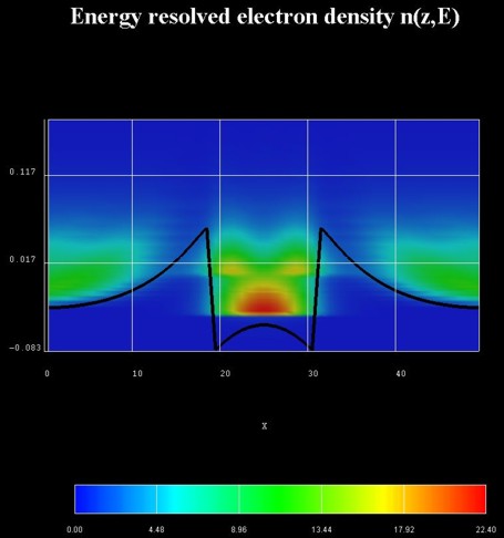
The figure on the left shows a contour plot of the energy resolved electron
density in the same situation as above, but this time including scattering fully
self-consistently. All phonon scattering mechanisms are fully included.
The lowest well state is a true bound state whereas the second one is a
resonance state an electron can tunnel out from into the leads.
Integrating n(z,E) over the energy E yields the electron
density n(z) which is shown in the
following figure, including the self-consistently calculated conduction band
edge. The Fermi level EF is also
shown.

NEGF calculation including scattering - 150 mV bias
-> 1DNEGF_InGaAs_QW_scattering_bias.in
Acoustic (both, elastic and inelastic) and polar-optical phonon scattering, electron-electron scattering in
Hartree approximation, see Fig. 1 (b) and 2 (a) in [Kubis_HCIS14_2005].
- VSD = 0.150 eV (source-drain), see Fig. 2 (a) in
[Kubis_HCIS14_2005].
Results
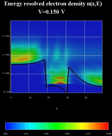
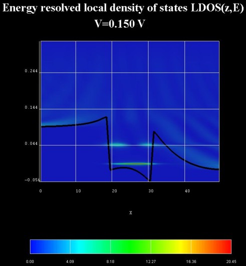
The following two figures show the energy resolved electron density and the
energy resolved local density of states for the QW under an applied bias of
0.150 V.
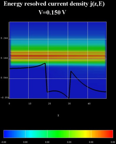
The following figure shows the energy resolved current density j(z,E)
in units of [Ampere/(cm^2 eV)].
The relevant data is contained in these files:
NEGF/EnergyResolvedCurrent_avs.v / *.dat / *.coord / *.fld.
The following figure shows the self-consistently calculated conduction
band profile and the electron density n(z).

Boundary conditions for the Poisson equation
 $global-parameters-NEGF

  ...

  !----------------------------------------------------------------------

  ! for Poisson equation: flat band boundary condition

  ! ==> Neumann boundary condition: d phi / d z = 0

  !----------------------------------------------------------------------

  given_slope   = yes       !
The slope of the poisson potential at the contacts is fixed: flat
band
  poisson_slope = 0d0       ! [V/Angstrom]


  chemical_potential = 0d0  ! [eV]
  zero_drift         =
yes  ! yes =
Grid points - Resolution
 $global-parameters-NEGF

  grid_points_in_z  =  50
!
number of grid points in real space along z direction.
! It must hold: nextnano3 grid points - 1 = grid_points_in_z
grid_points_in_E = 80
! E = total energy
grid_points_in_Ez = 120 ! k|| Ez = E - hbar2 * k||2
/ [2m(1)], 1 = 1st grid point
Applied bias (a voltage sweep is optional)
 $poisson-boundary-conditions


  !----------------------------------------------------------------

  !
Note: For NEGF, the voltage sweep applies to the left contact.
  !----------------------------------------------------------------

  poisson-cluster-number  = 1
!
  region-cluster-number   = 1
!
 !applied-voltage         =
0.0d0    ! 0
V           ! [V]
  applied-voltage         = 0.150d0
! 0.155 V = 150 mV  ! [V]
  boundary-condition-type = ohmic

  contact-control         =
voltage


  poisson-cluster-number  = 2
!
  region-cluster-number   = 4
!
  applied-voltage         =
0.0d0    ! 0 V
! [V]
  boundary-condition-type = ohmic

  contact-control         =
voltage
This keyword is necessary in order to loop over different voltages.
 $voltage-sweep

  sweep-number
= 1
!

  sweep-active
= no        ! 'yes'/'no'

  poisson-cluster-number = 1
! Note: For NEGF, the voltage sweep applies to the left contact.

  step-size
= 0.010d0   ! [V]    0.010
V = 10 mV

  number-of-steps        =
5 !
Chemical potentials (often called Fermi levels) at the contacts:
==>
! applied-voltage = 0.0d0

==>
left contact = right contact + e * applied voltage
! applied-voltage = 0.150d0

(preliminary, has to be generalized!)
|