|
| |
nextnano3 - Tutorial
next generation 3D nano device simulator
1D Tutorial
Density in np-doped GaAs superlattice - Comparison of classical, quantum, k.p and
full-band density k.p approach for normal and broken gap alignment
Author:
Stefan Birner
Please send comments to support (-at-) nextnano.com.
If you want to obtain the input file that is used within this tutorial, please
submit a support ticket.
a)

==> Density_GaAs_np_doped1D_cl.in
-
classical density
==> Density_GaAs_np_doped1D_qm.in
-
==> Density_GaAs_np_doped1D_qm_kp.in
-
==> Density_GaAs_np_doped1D_qm_kp_fullband.in -
==> Density_GaAs_np_doped1D_qm_kp_fullband_hl.in -
b)

==> Density_GaAs_np_doped1D_broken_cl.in
-
==> Density_GaAs_np_doped1D_broken_qm.in
-
==> Density_GaAs_np_doped1D_broken_qm_kp.in
-
-
not possible !!!
==> Density_GaAs_np_doped1D_broken_qm_kp_fullband.in -
==> Density_GaAs_np_doped1D_broken_qm_kp_fullband_hl.in -
Density in np-doped GaAs superlattice - Comparison of classical, quantum,
k.p and full-band density k.p approach for normal and broken gap alignment
The aim of this tutorial is to compare the density calculation of different
methods that are implemented in the nextnano³ software with respect to a
broken gap situation.
It is a self-consistent Schrödinger-Poisson calculation.
This tutorial is similar to the discussion in
Self-consistent electronic structure method for broken-gap superlattices
T. Andlauer, T. Zibold, P. Vogl
Proc. SPIE
7222, 722211 (2009)
As an example, we use an np-doped bulk GaAs superlattice of periodic length 20 nm with
periodic boundary conditions for the Schrödinger and Poisson equations.
- The temperature is set to 300 K.
- n-type region: 5 nm - 15 nm
- p-type region: 0 nm - 5 nm and 15 nm to 20 nm
-
n-type: The donor concentration is 5.2 x 1019 cm
-3
(fully ionized).
- a) normal band alignment: p-type: The
acceptor concentration is 2.6 x 1019 cm
-3
(fully ionized)
b) broken gap band alignment: p-type: The acceptor concentration is 5.2 x 1019 cm-3
(fully ionized)
- In order to compare the 8-band k.p results to the simpler models for
the density, we assume for all k.p calculations a parabolic and
isotropic energy dispersion E(k) of electrons and holes where
electrons and holes are decoupled. To achieve this, we use the following
parameters:
EP = 0 eV
S = 1/me = 1/0.067
L = M = -3, N = 0 (or equivalently: gamma1 = 2,
gamma2 = gamma3 = 0)
mhh = mlh = mso = 0.5 m0
- The number of grid points is 41, leading to a grid spacing of 0.5 nm.
a) normal band alignment, positive band gap Eg > 0, Ec
> Ev
The following figure shows the self-consistently calculated conduction band
edge Ec and highest valence band edge Ev for the normal
band alignment, i.e. positive band gap Eg.
EF is the Fermi level. The p-type doped regions are indicated in
grey, the n-type region in white.
These results are identical for single-band calculation, 8-band k.p
calculation and full-band k.p calculation for electrons.
For full-band k.p calculation for holes, the only difference is
that the electron density is zero, and that the hole density contains a negative
charge density which is equal to the shown electron
density, apart from the sign.
The classical calculation differs slightly. This is expected, since the
structure represents a quantum well like structure exhibiting confinement and
wave function penetration into the barrier.

The electron density is contained in this file:
densities/density1Del.dat
The hole density is contained in this file:
densities/density1Dhl.dat
(for full-band density for holes)
b) broken band alignment, negative band gap Eg < 0, Ec
< Ev
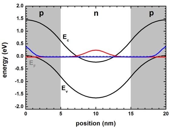
The following figure shows the results of the full-band k.p calculation where
the band gap Eg of conduction to valence band edge alignment is
negative.
The electron density is shown with positive sign (although it is of course
negative in reality) so that this figure can be easier compared to the above one
for normal band gap alignment.
If the density is negative as in the p-type region, it corresponds to hole
density (which is of course positive in reality).

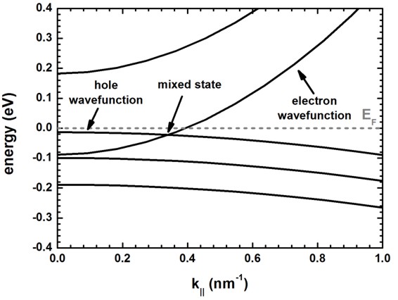
The following figure shows the energy dispersion E(k||).

In this figure, one cannot classify the energy states into pure electron and
hole states as at certain wavevectors also mixed states occur.
In fact, this is not really true for this example.
In this example, we set the Kane parameter EP to zero, i.e. we
decoupled electron states from hole states.
In this case we cannot get mixed states. We can only get electron states and
hole states that have similar energy.
This is shown in the next figure which shows the
square of the electron wave function (electron eigenvalue number 243
and 244, two-fold spin-degenerate),
and the square of the hole wave functions
("electron" eigenvalue number 245, 246, 247, 248, two-fold spin-degenerate, and
light hole / heavy hole degenerate due to choice of k.p parameters)
for k|| number 9. The kx and ky values for this
k|| number can be obtained from this file.
Schroedinger_kp/kp_8x8k_parallel_qc001_el1D_per.dat


k_par_number  k_x[1/Angstrom]  k_y[1/Angstrom]

...

9
0.0181818        0.0272727


k = (kx2 + ky2)1/2 =
0.0328 [1/Angstrom] = 0.328 [1/nm]
The electron eigenvalue is below the "hole" eigenvalue energy in this
figure.
For higher k|| vectors, this electron eigenvalue energy will be above
the hole energy eigenvalue.

In the full-band density k.p approach, both the
red and the blue eigenstate will
be occupied as an electron state.
By subtracting a positive background charge density, one gets the final density
distribution.
Full-band-density (8-band k.p)
The following switch is required to turn on "full-band density".
$numeric-control

 ...

 broken-gap = full-band-density
As the structure consists of 41 grid points, we get 8 x 41 = 328 eigenstates
for 8-band k.p in total.
Normal band gap situation:
The lowest 6 x 41 = 246 eigenstates belong to the hole states with their
energies below the valence band edge.
There are 2 x 41 = 82 electron states above the conduction band edge.
- full-band density for electrons:
$quantum-model-electrons
Here, we calculate all hole states, and the relevant electron states (number-of-eigenvalues-per-band
= 40),
i.e. we need the eigenstate numbers 1 - 286, where 286 = 246 + 40.
For the output, we plot only 235 -
278, i.e. the highest 12 holes states are included in the
output of the wave functions.
cb-num-ev-min = 235 ! lower
boundary for range of conduction band eigenvalues
cb-num-ev-max = 278 !
All eigenstates are treated as electrons, and occupied as
electrons, and contribute to the (negative) electron
charge density.
We then subtract a positive background charge density to obtain the
final net charge density.
The file
densities/density1Del.dat
contains the electron charge carrier density which is positive in this
example because a net electron density is present.
- full-band density for holes
$quantum-model-holes
Here, we calculate all electron states, and the relevant hole states (number-of-eigenvalues-per-band
= 40 40 40),
i.e. we need the eigenstate numbers 1 - 122, where 122 = 82 + 40.
For the output, we plot only 77 -
100, i.e. the 6 lowest electron states are included in the
output of the wave functions.
vb-num-ev-min = 77 ! lower
boundary for range of valence band eigenvalues
vb-num-ev-max = 100 !
We then subtract a negative background charge density to obtain the
final net charge density.
The file
densities/density1Dhl.dat
contains the hole charge carrier density which is negative in this
example because a net electron density is present.
Full-band-density holes ($quantum-model-holes)
is recommended, as one has less eigenvalues to calculate. This will make the
numerical effort smaller.
|