— FREE — Finite Periodic Structures
Header
- Files for the tutorial located in nextnano++\examples\basics
basics_1D_finite_periodic_simple.in
basics_1D_finite_periodic_double.in
Introduction
We will now concentrate on two particular features inside the structure{ }
group which enable you to create periodic structures conveniently. We will discuss their application
at the example of a finite superlattice structure. After completing this tutorial, you will know more about
creating periodic structures with
array_x{}duplicating periodic structures with
array2{}
Keywords: array_x{}, array2{}
Main
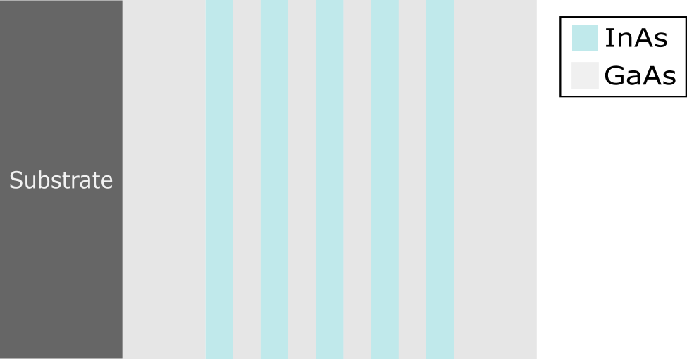
In the first part, we want to show how to create the structure in Figure 2.4.5.

Figure 2.4.5 shows multiple GaAs/InAs quantum wells, which forms a finite superlattice
In the second part, we extend the input file of part one, and create the structure shown in Figure 2.4.6.

Figure 2.4.6 shows a sequence of three GaAs/InAs superlattices
Based on what we learned in tutorial 1, we should have the basic knowledge to create these structure without using arrays. It would be quite an effort to create layer by layer. arrays offer a convenient alternative to that approach. The idea is to duplicate an existing sample structure multiple times in a specific direction. This takes just a few lines of code and gives in addition much more flexibility for your simulations. The sample structure in our case will be the GaAs/InAs/GaAs heterostructure from tutorial 1.
Input file 1: Repeated regions
Specifying the structure of the device
19structure{ # this group is required in every input file
20    region{
21        binary{ name = GaAs }           # material: GaAs
22        contact{ name = whatever }      # contact definition
23        everywhere{}                    # ranging over the complete device
24    }
25    region{
26        binary{ name = InAs }           # material: InAs
27        line{ x = [ 20.0, 30.0 ] }      # ranging from x=20.0 nm to x=30.0 nm, overwrites the previously defined GaAs
28
29        array_x{                        # line{ x = [ 20.0, 30.0 ] } is duplicated in the x direction
30            shift = 20.0                # the interval  x = [ 20.0, 30.0 ] inside line{} is shifted by an integer multiple of 20.0 nm
31            max = 2                     # 2 duplicates in +x direction
32            min = -2                    # 2 duplicates in -x direction
33        }
34
35        # In short, we are creating 5 InAs regions (overwriting GaAs) in the intervals:
36        # line{ x = [20.0+i*shift, 30.0 nm+i*shift]} (min<=i<=max)
37    }
38}
As in tutorial 1, we create an InAs layer, which ranges from \(x = 20 \text{nm}\) to \(x = 30 \text{nm}\).
By introducing array_x{} this layer is duplicated along x.
The position of the duplicates is determined by the shift value.
The shift direction (\(+x\) or \(-x\)) and the number of duplicates in each direction is set by max and min.
Here, max=2 creates two duplicates in the \(+x\) direction every \(20\text{nm}\).
The first “copy” ranges from \(x = 20\text{nm}+\mathbf{1}\cdot20 \text{nm} = 40 \text{nm}\) to \(x = 30\text{nm}+\mathbf{1}\cdot20 \text{nm} = 50 \text{nm}\) and
the second ranges from \(x = 20\text{nm}+\mathbf{2} \cdot 20 \text{nm} = 60 \text{nm}\) to \(x = 30\text{nm}+\mathbf{2} \cdot 20 \text{nm} = 70 \text{nm}\).
Analogous, min=-2 creates two duplicates in the \(-x\) direction every \(20\text{nm}\). Mind the negative sign!
After defining the structures, we have to adapt the grid to our newly constructed device.
Specifying the grid
40grid{ # this group is required in every input file
41    xgrid{                  # grid in x direction
42        line{
43            pos = -40.0     # start device at x=-40.0 nm
44            spacing = 4.0   # grid spacing 4.0 nm
45        }
46                            # from x=0.0 nm to x=20.0 nm further grid points
47                            # are created according to the interpolated spacing (4.0 -> 0.5)
48                            # (no equidistant grid spacing)
49        line{
50            pos = -20.0     # bottom GaAs/InAs interface at x=-20.0 nm
51            spacing = 0.5   # grid spacing 0.5 nm
52        }
53                            # from x=-20.0 nm to x=70.0 nm further grid points
54                            # are created according to the interpolated spacing (0.5 -> 0.5)
55                            # (equidistant grid spacing)
56        line{
57            pos = 70.0      # top InAs/GaAs interface at x=70.0 nm
58            spacing = 0.5   # grid spacing 0.5 nm
59        }
60                            # from x=70.0 nm to x=90.0 nm further grid points
61                            # are created according to the interpolated spacing (0.5 -> 4.0)
62                            # (no equidistant grid spacing)
63        line{
64            pos = 90.0      # start device at x=90.0 nm
65            spacing = 4.0   # grid spacing 4.0 nm
66        }
67    }
68}
We first extend the device, since we created new material regions: the bottom of the lowest InAs layer is located at \(x_min=-2 \cdot 20 \space \text{nm} +20\space \text{nm} = -20.0\space \text{nm}\) and the top of the highest InAs layer is located at \(x_min=30\space \text{nm} + \mathbf{2} \cdot 20 \space \text{nm} = 70 \text{nm}\). We have chosen \(x=-40\text{nm}\) and \(x=70\text{nm}\) as our start and end points, in order to include all new material layers. In tutorial 1 we have learned that we also have to take care about interfaces. To keep things simple, we use an equidistant grid spacing inside the superlattice.
Output
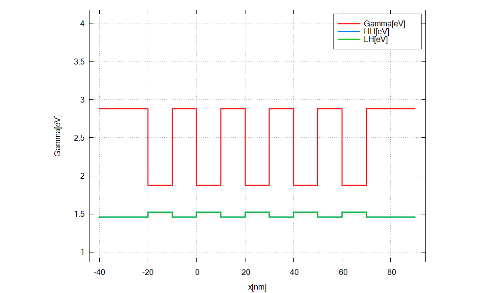
We simulate the device by clicking F8 on the keyboard. In the related output file (\(\Rightarrow\) bias_00000 \(\Rightarrow\) bandedges.dat) you should find a plot of band edges
as shown in Figure 2.4.7.

Figure 2.4.7 shows energy profile of multiple quantum well structure
Input file 2: Repeated structres
Specifying the structure of the device
19structure{ # this group is required in every input file
20    region{
21        binary{ name = GaAs }           # material: GaAs
22        contact{ name = whatever }      # contact definition
23        everywhere{}                    # ranging over the complete device
24    }
25    region{
26        binary{ name = InAs }           # material: InAs
27        line{ x = [ 20.0, 30.0 ] }      # ranging from x=20.0 nm to x=30.0 nm, overwrites the previously defined GaAs
28
29        array_x{                        # line{x=[20.0,30.0]} is duplicated in the x direction
30            shift = 20.0                # the interval  x = [ 20.0, 30.0 ] inside line{} is shifted by an integer multiple of 20.0 nm
31            max = 2                     # 2 duplicates in +x direction
32            min = -2                    # 2 duplicates in -x direction
33        }
34        # In short, we are creating 5 InAs regions at positons:
35        # line{ x = [20.0+i*shift, 30.0 nm+i*shift]} (min<=i<=max)
36
37        array2_x{
38            shift = 120.0               # the structure previously defined inside this region
39            max = 2                     # is duplicated and shifted by i*120 nm (1<=i<=max) in +x.
40        }
41    }
42}
We add the group array2_x{} which is used to duplicate the structure defined by array_x{} within the same region{}.
We get a sequence of periodic structures. The usage is analogous to array_x{}, thus it follows the same logic with shift, max and min.
Specifying the grid
45grid{ # this group is required in every input file
46    xgrid{                          # grid in x direction
47        line{
48            pos = -50.0             # start device at x=-50.0 nm
49            spacing = 4.0           # grid spacing 4.0 nm
50        }
51                                    # from x=-50.0 nm to x=-20.0 nm further grid points
52                                    # are created according to the interpolated spacing (4.0 -> 0.5)
53                                    # (no equidistant grid spacing)
54
55        line{                       # fixed grid points are created at the bottom GaAs/InAs interfaces of every multiple QW structure
56            pos = -20.0             # bottom GaAs/InAs interface at x=-20.0 nm
57            spacing = 0.5           # grid spacing 0.5 nm
58
59            array{                  # fixed grid point at x=-20 nm is duplicated (including spacing)
60                shift = 120.0       # shifted by 120.0 nm
61                max = 2             # two copies are created at x=-20.0 nm+i*shift (1<=i<=max)
62            }
63        }
64
65        line{                       # fixed grid points are created in the middle of two multiple QW structures to change grid spacing
66            pos = 85.0              # position: x=85.0 nm
67            spacing = 4.0           # grid spacing 4.0 nm
68
69            array{                  # fixed grid point at x=85.0 nm is duplicated (including spacing)
70                shift = 120.0       # shifted by 150.0 nm
71                max = 1             # one copy is created at x=85.0 nm+max*shift
72            }
73        }
74
75        line{                       # fixed grid points are created at the top GaAs/InAs interfaces of every multiple QW structure
76            pos = 70.0              # top InAs/GaAs interface at x=70.0 nm
77            spacing = 0.5           # grid spacing 0.5 nm
78
79            array{                  # fixed grid point at x=70.0 nm is duplicated (including spacing)
80                shift = 120.0       # shifted by 120.0 nm
81                max = 2             # two copies are created at x=70.0 nm+i*shift (1<=i<=max)
82            }
83        }
84                                    # from x=310.0 nm to x=340.0 nm further grid points
85                                    # are created according to the spacings (0.5 -> 4.0),
86                                    # which is interpolated (no equidistant spacing)
87        line{
88            pos = 340.0             # end device at x=340.0 nm
89            spacing = 4.0           # grid spacing 4.0 nm
90        }
91    }
92}
In this example, we show that method of arrays also exist for the grid{ }. Here, they are called array{}, but used equivalently to array_x{}.
They create copies of one fixed grid point, including the related spacing value.
Output
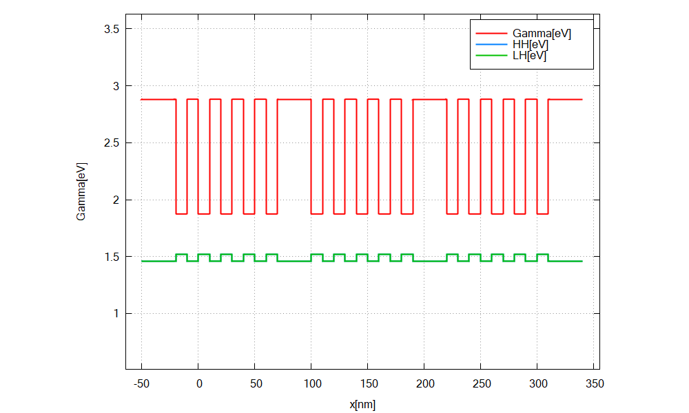
We simulate the device by clicking F8 on the keyboard. In the related output file you should find a plot of band edges
(\(\Rightarrow\) bias_00000 \(\Rightarrow\) bandedges.dat)
similar to Figure 2.4.8.

Figure 2.4.8 shows the band edges of conduction band at gamma point (Gamma), heavy hole (HH) and light hole (LH) of the complete structure
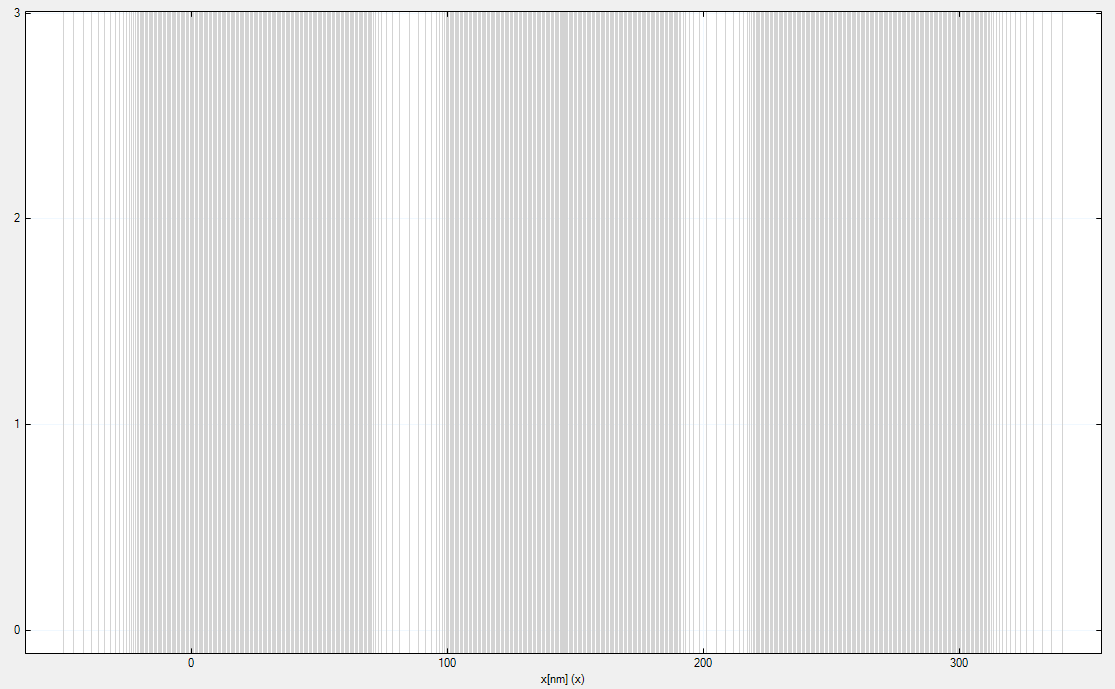
Just for demonstration, Figure 2.4.9 shows a screenshot of the employed grid.

Figure 2.4.9 Numerical grid (gray).
Important things to remember
Creating periodic structures works as follows: A special array of one template regions (here: one layer) is constructed
Position and number of new regions are determined by
shift,maxandminCreating a sequence of periodic structures with
array2{}works equivalently toarray{}Do not forget to adapt the grid to the complete structure. It is also possible to create an array of grid points.
Last update: 16/07/2024